

General Description
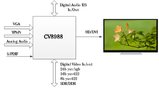
The CV8988 device is a high quality interface converter with analog video Front-end, analog audio Front-end and HD Transmitter.
The CV8988 device supports video signals up to 1080p60 and UXGA resolution.
The device contains a 24 Bits audio ADC, So CV8988 can accept three format audio signal: Digital audio S/PDIF and I2S, analog stereo Line in.
The video and audio TTL pin can defined as input and output. So the CV8986 can be used as:
Analog video and video to TTL
Analog video and audio to HD
Digital Video and Digital Audio to HD
Features
Analog Video Front-end
10-bit ADCs sampling up to 192Mhz
Flexible input multiplexers to support YPBPR, VGA and RGBS
Automatic format detection
Automatic position detection
Automatic gain and offset calibration
Automatic phase calibration
Digital Video input
Support 480i/p, 576i/p, 720p25/30/50/60, 1080i50/60, 1080p24/25/30/50/60
Support VESA mode from VGA to UXGA
Support 480i/p, 576i/p, 720p25/30/50/60, 1080i50/60, 1080p24/25/30/50/60
Support VESA mode from VGA to UXGA
Support SDR and DDR data rate
Support BT601/BT1120/BT656
Support 8-bit/16-bit/24-bit input
Analog Audio Front-end
Advance Multi-bit ΔΣ Architecture
24-bit Conversion
Supports Audio Sample Rates Up to 108Khz
Low-Latency Digital Filter
Digital audio interface
Four I2S inputs with sample rate of 32~192Khz
S/PDIF interface supporting PCM,Dolby Digital, DTS digital audio at up to 192Khz frame rate
Compatible with IEC 60958 and IEC 61937
HD Transmitter
HD 1.3/DVI 1.0 compliant transmitter up to 170Mhz, supporting 1080p and UXGA.
Monitor detection
Digital Video output
Support SDR and DDR data rate
Support BT601/BT1120/BT656
Support 8-bit/16-bit/24-bit input
Packaging
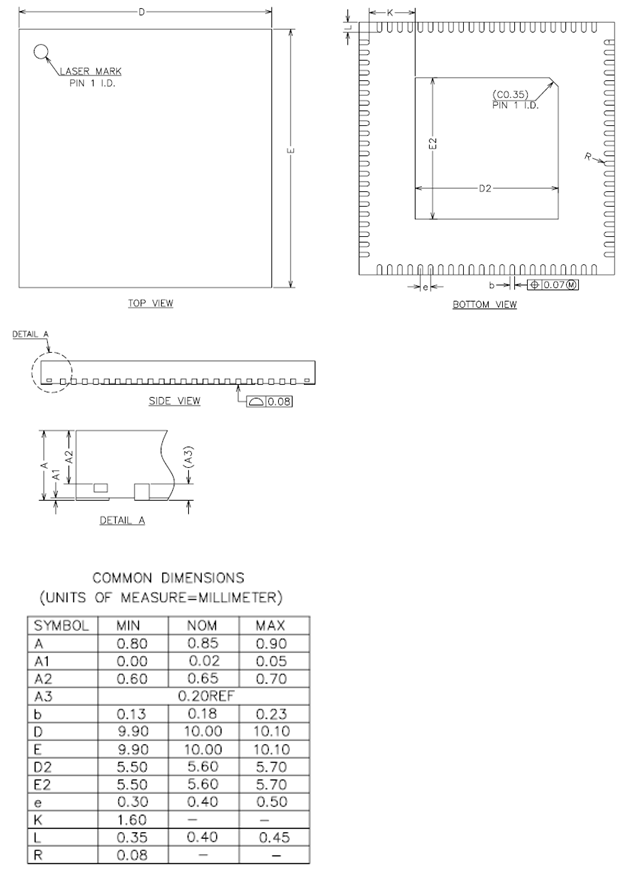
88 pin plastic QFN,Size 10mmX10mm.
Application
Pin Diagram
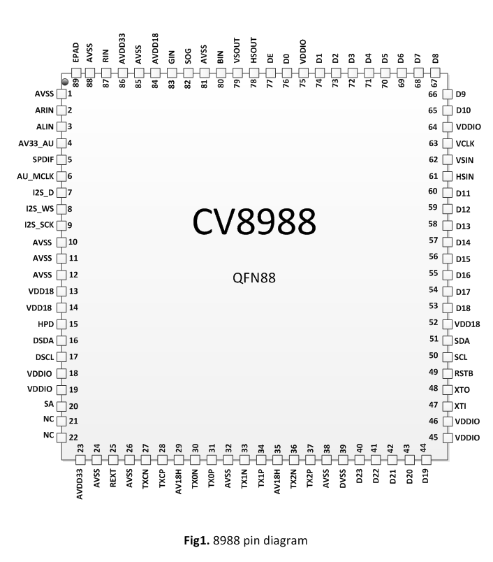
Pin Description
| PIN | Signal Name | Type | Dir | Description |
| 1 | AVSS | Ground | P/G | Ground |
| 2 | ARIN | Analog | Input | Line Input for Right Channel. |
| 3 | ALIN | Analog | Input | Line Input for Left Channel. |
| 4 | AV33_AU | Power | P/G | Analog Power 3.3V |
| 5 | SPDIF | Schmitt | Input | S/PDIF Audio Input. |
| 6 | AU_MCLK | Schmitt | Input/Output | Audio Master Clock. |
| 7 | I2S_D | Schmitt | Input/Output | I2S Serial Data. |
| 8 | I2S_WS | Schmitt | Input/Output | I2S Word Select. |
| 9 | I2S_SCK | Schmitt | Input/Output | I2S Serial Clock. |
| 10,11,12 | DVSS | Ground | P/G | Ground |
| 13,14 | VDD18 | Power | P/G | Digital power 1.8V |
| 15 | HPD | Schmitt 5-V tolerant | Inpput | Hot Plug Detect Input. |
| 16 | DSDA | Schmitt Open-drain 5-V tolerant | Input/Output | DDC I2C Bus Data. |
| 17 | DSCL | Schmitt 5-V tolerant | Input/Output | DDC I2C Bus Clock. |
| 18,19 | VDDIO | Power | P/G | Digital IO power 3.3V |
| 20 | SA | Schmitt | Input/Output | I2S ADDRESS Select. |
| 21,22 | NC | |||
| 23 | AVDD33 | Power | P/G | Analog Power 3.3V |
| 24 | AVSS | Ground | P/G | Analog Ground |
| 25 | REXT | Analog | Input | Voltage Swing Adjust.A resistor is connected from this signal to GROUND.This resistor determines the amplitude of the voltage swing. |
| 26 | AVSS | Power | P/G | Analog Ground |
| 27 | TXCN | TMDS | Output | TMDS output clock pair. |
| 28 | TXCP | TMDS | Output | |
| 29 | AV18H | HD TX 1.8V Power | ||
| 30 | TX0N | TMDS | Output | TMDS ouptut data0 pairs. |
| 31 | TX0P | TMDS | Output | |
| 32 | AVSS | Ground | P/G | Analog Ground |
| 33 | TX1N | TMDS | Output | TMDS ouptut data1 pairs. |
| 34 | TX1P | TMDS | Output | |
| 35 | AV18H | Power | P/G | HD TX 1.8V Power |
| 36 | TX2N | TMDS | Output | TMDS ouptut data1 pairs. |
| 37 | TX2P | TMDS | Output | |
| 38 | AVSS | Ground | P/G | Analog Ground |
| 39 | DVSS | Ground | P/G | Ground |
40,41,42,43,44,53,54, 55,56,57,58,59,60,65, 66,67,68,69,70,71,72, 73,74,76 | D | Schmitt | Input/Output | Digital Video data IO |
| 45,46 | VDDIO | Power | P/G | Ground |
| 47 | XTI | Crystal Input. | ||
| 48 | XTO | Crystal Output. | ||
| 49 | RSTB | Schmitt | Input | Reset signal(active LOW) |
| 50 | SCL | Schmitt | Input | Serial Port Data Clock |
| 51 | SDA | Schmitt Open drain | Input/Output | Serial Port Data I/O |
| 52 | VD18 | Power | P/G | Digital Power 1.8V |
| 61 | HSIN | Schmitt 5-V tolerant | Input | Horizontal Sync Input |
| 62 | VSIN | Schmitt 5-V tolerant | Input | Vertical Sync Input |
| 63 | VCLK | Schmitt | Input | Video pixel clock Input |
| 64 | VDDIO | Power | P/G | Digital IO power 3.3V |
| 75 | VDDIO | Power | P/G | Digital IO power 3.3V |
| 77 | DE | Schmitt | Output | DE Output |
| 78 | HSOUT | Schmitt | Output | Horizontal Sync Output |
| 79 | VSOUT | Schmitt | Output | Vertical Sync Output |
| 80 | BIN | Analog | Input | Analog Input for Blue/CB Channel |
| 81,85,88 | AVSS | Ground | P/G | ADC Ground |
| 82 | SOG | Analog | Input | Sync-on-Green Input |
| 83 | GIN | Analog | Input | Analog Input for Green/Y Channel |
| 84 | AVDD18 | Power | P/G | Analog 1.8V |
| 86 | AVDD33 | Power | P/G | Analog 3.3V |
| 87 | RIN | Analog | Input | Analog Input for Red/CR Channel |
| 89 | EPAD | Ground | P/G | EPAD,Connect to Ground |
Packaging
更多产品
在线咨询
如果您对我们的产品有任何兴趣,欢迎随时给我们留言
联系芯成微,寻找集成电路系统方案。
地址:合肥市高新区创新大道2800号创新产业园二期F3栋1605、1606室

 0551-66691058
 tina.chen@chipsvi.com
  在线留言
在线留言


Copyright © 2021 合肥芯成微科技有限公司 版权所有. 皖ICP备18012159号


